Custom Porous Alumina Shapes for Semiconductor Fabrication
Why Specify Porous Alumina
✓ 99.9% ultra-high purity formulations are inert in extreme environments.
✓ Usable up to 1700°C
✓ Cleanable
✓ Pore sizes can be tailored to meet strength and flow requirements.
Why Choose Refractron?
✓ Experience developing, manufacturing, and testing custom 85-99.9% porous alumina
parts for semiconductor chip manufacturing.
✓ Dedicated production cell with a class 10,000 clean room
✓ Bolster your supply chain with a privately owned, domestic manufacturer.
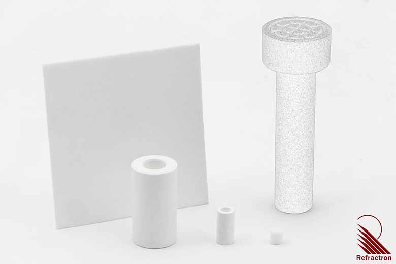
Refractron manufactures 85-91% glass bonded and ultra-high purity 99.9% custom porous alumina shapes that help eliminate unwanted contamination, improve yields, and improve process reliability in harsh environments. Custom high purity shapes can be designed with pore sizes from 0.1 to 1000 microns. The typical porosity of these formulations ranges from 28-45%.
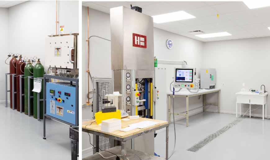
Our semiconductor production cell features a modern press, furnaces that operate to 1800°C and a class 10,000 clean room. Our team of engineers and scientists can collaborate on material selection, product design, quality control and performance testing to ensure process goals can be met. Tight dimensional tolerances can be realized with the right tools and help from our in-house 20,000 square foot grind shop.
Semiconductor Resources
✓ Refractron Advanced Porous Ceramic
✓ Porous Sintered Alumina Filters SAF0.3

How Can We Help You?
Contact Adam Osekoski, Vice President of Sales & Marketing at Refractron +1 315-573-1134, adamo@refractron.com to learn if Refractron’s team of engineers and porous manufacturing experience can help you improve process reliability, reduce contamination, and extend the service of your critical equipment. Adam is a ceramic engineer with over 25 years of experience design, manufacturing and selling ceramics into critical applications like those found in the semiconductor industry.


